
SemiAnalysis disassembled to 9030: the process is blocked and the path is folded
Export controls had not prevented China from making progress on the chip, but had changed the path and cost of progress. 。
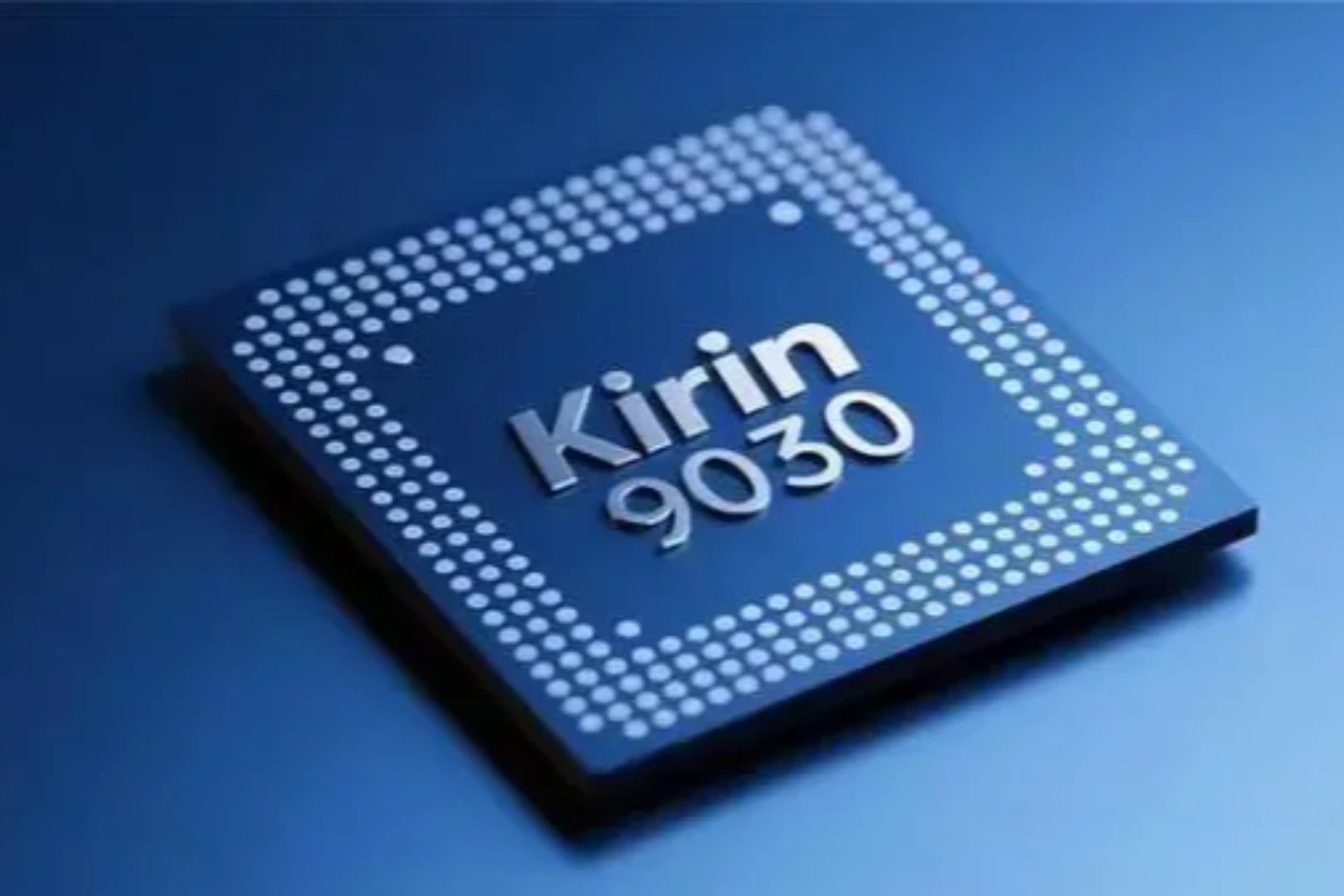
In the area of semiconductor reverse engineering, TechInsights ruled for decades. Last weekend, SemiAnalysis of Dylan Patel officially released the first public dismantling report of the STEEL Laboratories under the flag, targeting one of the world ' s most interesting chips, the unicorn 9030 Pro carried by China 80 Pro, using the state-of-the-art N+3 formula。
The timing is interesting. TechInsights are being sold for private equity, and SemiaAnalysis has earned more than this old giant. Dylan chose to light the sword in this node, using a highly technical decomposition report, in conjunction with a real chip photograph from the Oregon State Laboratory。
The title of the report is a bomb:The minimum metal spacing (M0 pitch) of SMIC N+3 is 32.5 nm, which is smaller than the 36 nm of the 18A program used by the latest Panther Lake processor in Intel。
Central International, without an EUV calculator, did the metal space get much smaller than Intel
This message, if you look only at the title, is enough to blow up the whole semiconductor ring, but SimiAnalysis threw cold water himself in the second paragraph of the report, a "cherry picked metric" and a deliberately selected indicator。
This paper will be used to read the dismantling report
Density level-out, high cost
SMIC'S N+3 PROCESS IS ON TRANSISTOR DENSITY, AND DOES TRACK DOWN THE N6 OF THE BUILDUP。
The STEEL laboratory measured the Bohr density of N+3 at 113.4 Mtr/mm2, slightly higher than the TEM transverse analysis, which was 107.7 Mtr/mm2 of N6. The unit height is reduced from 252 nm at N+2 to 228 nm, and the contact grid polar spacing (CGP) from 63 nm to 57 nm. These numbers, taken together, mean that SMIC matures the level of 7 nm with the logical density by pure DUV light。
What's the price
THE SMIC M0 LAYER USES THE SELF-DIRECTED QUADRILATERAL MAPPING (SAQP), I.E. THE FOUR-TIME PROCESSING OF A MASK TO ACHIEVE A MORE REFINED LINE. ACCUMULATION N6 ON THE SAME FLOOR REQUIRES ONLY DOUBLE MAPPING (SADP). THE FOUR WEIGHTS MEAN MORE PHOTO MASKS, HIGHER SET ACCURACY REQUIREMENTS, MORE COMPLEX PROCESSES AND HIGHER COSTS。
SemiAnalysis sees the cost of SAQP directly in the cross-section: the M0 groove of N+3 shows a clear rewinding contours (the bottom is narrower than the top) and the bottom of the groove has a clear barrier zone. This shape, while contributing to copper filling, increases the difficulty of process control at this distance of 32.5 nm。
A TRADER CAN UNDERSTAND THE METAPHOR: SMIC IS MAKING BANKNOTES WITH THE SAME DENOMINATION, BUT THE COST OF PRINTING EACH ONE IS SEVERAL TIMES THE AMOUNT OF ELECTRICITY ACCUMULATED ON THE TABLE AND IS MORE RISKY. LIKE DENSITY, ECONOMICS IS COMPLETELY DIFFERENT。
Oxygen 9030: Under restricted conditions, every inch of silicon is drained
The design capability of Heath's chip is another dimension story。
From the size of the chip, thorium 9030 is almost as big as the previous generation 9020 (about 140mm2), but more stuff is inserted inside: CPU upgrades from one large nuclear + 3 to one large nuclear + 4, GPU computing units from four to six, and NPU has an additional Tiny core, with a full cache of all levels. The N+3 density increase allowed China to install more logical units in the same chip size。
In terms of performance, STEEL refers to open rundown data and gives a clear position: the gill 9030 GPU performance (Mareoon 935) has roughly reached the 2022 flagship level, with 3D Mark WLE running 70% higher than the previous generation, slightly exceeding the tiara 8+Gen 1, but the gap is 2.4 to 2.6 times higher than the current gill dragon 8 Elite Gen 5。
The CPU situation is more illustrative. TaiShan Prime's hourly performance (IPC) is approximately at Arm Cortex-X2 level, a 2021 design. Apple released the M1 Firestorm core in 2020, IPC is still 35% higher. The latest Apple M5P core, IPC, 60% higher, is 2.7 times more absolute。
THE ROOT CAUSE OF THE GAP IS NOT DESIGN, BUT PROGRAMMING. APPLES AND HIGH COMMONS ARE THE BUILD-UP N4, N3PS, WHICH HAVE A SUBSTANTIAL ADVANTAGE IN THE VOLTAGE-FREQUENCY CURVE: THE SAME AREA CAN BE PLUGGED INTO MORE TRANSISTORS AND THE SAME AMOUNT OF POWER CAN RUN HIGHER FREQUENCIES. THE CORE DESIGN LEVEL FOR CHINA IS MARKED BY THE FIRST GENERATION OF INDUSTRY, BUT TRAPPED IN TWO GENERATIONS OF PREVIOUS MANUFACTURING PROCESSES。
When the process stops, Wigand prepares to fold
The most forward-looking part of the report is the Law of China and the LogicFolding Road Map, published at the 2026 IPSAS Conference。
the traditional semiconductor indentation moves on a 2d plane: small transistors, fine metal lines. moore's law has been gone for decades, and it's basically doing it. china scaled up the current proposal to shift the optimization target from a spatial domain to a temporal domain centred on reducing the time costs of data movement and processing, including delays in transistor switches, delay in signal transmission, delay in computing and storage。
LogicFolding is the realization of this theory. In short, the same logical module is broken down into two layers, stacked face-to-face, and connected by a hybrid of supersample spacing. The immediate advantage of this is to shorten the longest signal path. A significant portion of the current chip is spent on driving long-wire and trunk buffers. When the logic is folded vertically, the key path becomes shorter, the frequency can go up and the effort can come down。
Wigand gave us a radical road map:The large nuclear frequency of thorium 9030 is 2.75 GHz, which runs through a sample of 3.39 GHz in the laboratory. The goal is to reach 5 GHz by 2031, while the equivalent density is pushed to 295 MTr/mm2 by stacking of 3D, with 14A levels of electricity to the standard table。
SemiAnalysis is vigilant about this. They pointed out that the method of calculating China ' s density was different from the traditional plant: The density of 3D stacks is based on the size of the encapsulation, which puts multiple layers of dynamic logic together and naturally leads to higher numbers. If AMD's MI450X (N2 Top + N3P Bottom) are calculated in the same way, the theoretical density is as high as 460.2 Mtr/mm2, far above the 2031 target。
But the direction itself deserves attention. In order to go this way, China essentially took over the work of the substitute factory to the system design company with limited programming. The AMD V-Cache stacks 3D on the cache, AMD MI350X moves IO and interconnection to the bottom chip, and Wigand is going to do it more thoroughly, tearing up the same logic block directly, vertically, which is another quantitative challenge in terms of engineering difficulty。
Export controls reshaped the dimensions of the competition
SemiAnalysis concludes:Export controls had not prevented China from making progress on the chip, but had changed the path and cost of progress。
The SMIC N+3 certificate does not use EUV to achieve N6 level logical density. But this road is more costly, more complex processes and more difficult to control. Moving down, the marginality of each step is increasing: more masks, stricter engraving precision, more expensive multiple mapping. Theoretically, N+4 can do 137.8 Mtr/mm2 (to build N5), N+5 can even approach the HP library of Intel 18A by adding back power. But each step is more difficult, more expensive and less room for error than the previous one。
AT THE SAME TIME, THE SMIC N+2 AND N+3 PROCESSES ARE MOVING TOWARDS THE ZHUANG, AND DESIGN COMPANIES SUCH AS ALI PING-CHU AND CHIU-CHI ARE LIKELY TO BE BENEFICIARIES. THE SPREAD OF KNOWLEDGE IN CHIP MANUFACTURING FROM SINGLE-GENERATION PLANTS TO ECOSYSTEMS FURTHER DILUTES THE EFFECTIVENESS OF SANCTIONS AGAINST SINGLE ENTERPRISES。
At the design end, Wigand and Beijing University are already developing a prototype national EDA tool for LogicFolding. This does not replace the complete tool chain of Synopsys and Cadence, but the national EDA is moving in the direction of "structure-programming-covering synopsis"。
An interesting detail: STEEL found in the dismantling that the DRAM of 9030 Pro came from Tristar (K4L2E165YD, LPDDR5X-9600, 1a process node), while the Pro Max version of 16GB showed the cover of the Tristar and Longstar storage (CXMT). The sealed date of the long chip is marked 45th week of 2025, with a process density equivalent to that of industry 1z. This means that Chinese storage chips have begun to enter the Chinese flagship supply chain, although the production process is still lagging behind the three stars and the SK Hercules generation。
FOR INVESTORS, THE REAL SIGNAL TO FOLLOW LIES IN WHETHER THE 3D STACKING ROUTE BY CHINA WILL ALLOW CHINESE CHIPS TO REACH A CRITICAL MASS IN SUCH SCENARIOS AS MOBILE PHONES, AI REASONING, AND NETWORK EQUIPMENT, AT A MANAGEABLE COST。
Once sufficient, the strategic value of this supply chain is re-pricing。
